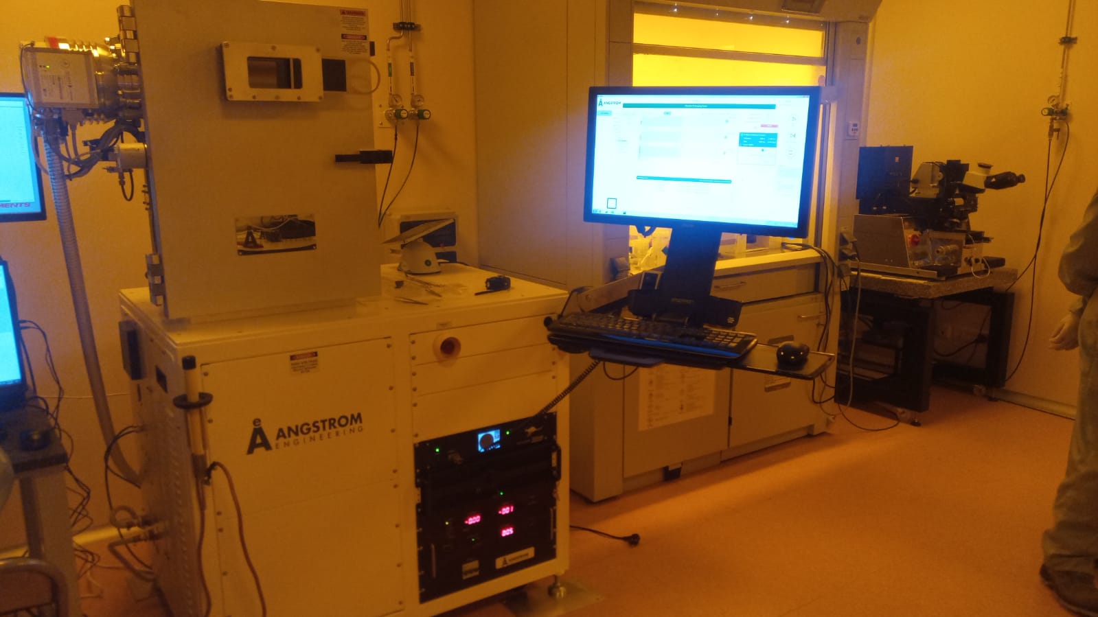
Electron beam physical deposition system

ELECTRON BEAM PHYSICAL DEPOSITION SYSTEM CAPABLE OF THIN FILM METALLIC, DIELECTRIC AND SEMICONDUCTOR MATERIAL DEPOSITION
Research institute: UPNA-Institute of Smart Cities
Manufacturer: Angstrom Engineering
Model: PVD-NEXDEP
Location: Sala Limpia. Edificio I+D Jerónimo de Ayanz. Campus Arrosadia. UPNA. Pamplona.
Associated technology services: UPNA has specialized infrastructure and technical expertise in micro- and nanofabrication, thin-film processing, and advanced surface characterization. We offer end-to-end R&D support—from initial proof-of-concept design and substrate patterning to functional device prototyping. Key capabilities include high-precision lithography, physical and chemical thin-film deposition, microstructuring, and high-resolution electron and atomic force microscopy.
Application sector: High-tech industries and strategic research domains. Our microfabrication and analytical capabilities directly support key sectors such as Smart Cities, advanced electronics, comunnications, microfluidics, biomedical devices (lab-on-a-chip platforms), environmental sensing and integrated photonics.